SAN JOSE, Calif — NVIDIA has cemented its central position in the technology industry over the last few years. It has the most in-demand products and amongst the biggest revenue and biggest market capitalization. It’s a once-in-a-lifetime moment for everyone involved, as the Talking Heads once sang, but the torrent of product releases is extremely hard to keep up with and make sense of.
There is an impressive amount of business agility and relentless progress, but sometimes headline-making announcements are quietly forgotten or superseded by even better products before people have had a chance to get their hands on them. NVIDIA is announcing new hardware that effectively obsoletes its previous products well before they are available, but customers are buying whatever they can get, as it appears.
Meanwhile “the new stack” of AI software is maturing rapidly, easy-to-use, pre-tuned, high-performance open source models are available, and a plethora of AI-based services and tools are competing for everyone’s attention. Development is also being accelerated by a variety of AI-backed tools that are improving rapidly.
Last year, I predicted that enterprise customers would find it extremely difficult to manage the pace of change, and get “enterprise indigestion,” but that hyperscalers would be happy. This year, I think the hyperscaler customers and cloud providers have indigestion as well. It takes a few years to plan and build a data center, but the specification of the racks and the power density keeps going up, so they must be replanning before they are finished building. NVIDIA is responding by releasing a very wide range of packaging options to target various points in the market and providing more information about its future roadmap, which helps but is making it even harder to keep track of what’s going on.
How Did We Get Here?
Before we can make sense of what was announced by Jensen Huang, the CEO of NVIDIA, in his annual GTC keynote Tuesday, we need to establish some context by looking back at previous keynotes and additional announcements over the last year. There is a big disconnect between the GPUs that most people are using now (the ones that just started shipping, but that most people haven’t used yet) and those that are being announced this week. I’ve summarized them here, with links to in-depth stories for people interested in more detail.
The GPU servers that most people are familiar with right now have two Intel CPUs and eight NVIDIA Hopper H100 GPUs as the nodes that can be clustered. They were announced three years ago and are the mainstream workhorse underpinning most of the AI-based products and services we use today.
Two years ago in his keynote, Jensen announced the Grace Hopper GH200 combined CPU/GPU architecture. Grace was the first CPU designed by NVIDIA and uses ARM architecture rather than Intel, with an NVlink interface to couple it directly to a slightly upgraded Hopper H200 GPU. While it shipped in volume, the GH200 one-to-one mix of CPU to GPU is the wrong ratio for many AI training customers, who wanted more of their dollars and power budget to be spent purely on additional GPU capacity. Most H200 GPUs are actually being delivered in the same kind of 8-way with two Intel CPU packages as the H100s.
GH200 was the first attempt at a new shared memory system architecture where the GPU is driving the NVlink cluster interconnect, and the CPUs are hanging on around the edge. This is reversed from conventional architectures where the CPUs are in the center (that’s what the C in CPU stands for!) driving interconnection traffic, and GPUs are attached to them.
The difference is that when an H200 GPU wants to send data to another H200 GPU in the same system in a cluster, it goes directly across NVlink. This is far faster than a traditional GPU sending via a PCI bus to an Intel CPU then over a network to another Intel CPU, then via PCI to the other GPU. However, when one Grace CPUs wants to communicate with another, the data passes through at least two Hopper GPUs to get there.
GH200 systems seem to be more suited to the HPC Supercomputer market than the much bigger AI training and inference market. NVIDIA told me in 2024:
“The largest early systems are in Supercomputing including the Swiss National Computer Center ‘Alps’ system, Los Alamos National Labs ‘Venado’, Texas Advanced Computing Center ‘Vista’ and the Jülich Supercomputing Centre’s JUPITER system with close to 24,000 GH200 Superchips. These systems and more will be coming online throughout 2024. Combined, these GH200-powered centers represent some 200 exaflops of AI performance to drive scientific innovation.”
Blackwell GPU
In 2024, Jensen announced the Blackwell architecture GPU and the GB200 system. To get around limitations in the maximum size of chips that can be made, the Blackwell GPU is made from two of the largest possible chips, connected directly together. One Grace CPU is combined with two Blackwell GPU packages to make a GB200 node (addressing the issue with the 1:1 CPU/GPU ratio in GH200).
Blackwell GB200 modules have around four times the silicon area dedicated to GPU, and the same area for CPU, compared to GH200 modules. Two modules fit on a 1 rack-unit-high, water-cooled motherboard, and 18 compute boards fit in a 72 GPU NVL72 rack, along with switchboards to interconnect them.
NVIDIA has introduced several variations of the Blackwell and packaging options since launch, including a reduced-performance single-chip B200A variation that can be configured to be air-cooled as part of its MGX line of products. In the MGX GB200A NVL36 rack, each board takes two rack units and has a single Grace CPU resulting in a 9-CPU/36-GPU rack that needs 40kW of cooling, which is still a challenge but is easier to deploy in existing data centers.
At the end of 2024, it was disclosed that a new process from chip supplier TSMC allows for 50% higher performance Blackwell Ultra – B300 GPUs. These also use even more power, pushing the NVL72 rack from 132kW to 163kW, but it appears that many of the orders and plans that were in place for B200 have now switched to Blackwell Ultra.
It also has more flexibility in its design options, allowing customers like AWS to customize its deployments to integrate with its custom packaging and network architecture. The Blackwell Ultra provides a rack-compatible upgrade to the NVL72 so that existing installations can extend their lifespan, and work done on productizing data centers to support the original NVL72 rack isn’t wasted.
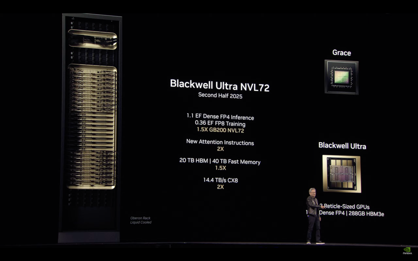
NVIDIA revealing Blackwell Ultra NVL72 onstage at GTC.
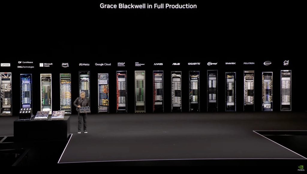
The highly structured AWS cloud architecture doesn’t naturally support dropping in a product like NVL72, and while Blackwell GPUs are available from cloud providers including Azure in late 2024, Google Cloud in January 2025, and Coreweave, the latest AWS GPU that is generally available as of March 18, 2025 is the p5 that has eight H200 with two Intel CPUs. Amazon Web Services is currently only shipping Blackwell privately to its biggest customers. In the header shot for this story, you can see the variants of Blackwell-based racks that are deployed by each provider.
Looking closely, it appears that most of the racks including Azure and Oracle cloud are NVL72, but AWS and GCP are using the air-cooled MGX36, and HP has its own custom Cray architecture rack for HPC that hosts 244 Blackwell GPUs. I haven’t seen any new announcements from AWS at GTC and confirmed that it has no announced Blackwell-based products right now after visiting its expo booth. And you may ask yourself, how did they get here?
There was already some disclosure in mid-2024 but Jensen provided more details of the next-generation 2026 Vera CPU and Rubin GPU, which has even higher per-rack power requirements. To reduce “hyperscaler indigestion,” the first version of Rubin also delivers into the same NVL72 rack architecture, with another bump in power consumption and a change in naming convention to Vera Rubin NVL144. Jensen said that they are reverting to calling a two-die module two GPUs for Rubin rather than one, as Blackwell was too confusing.
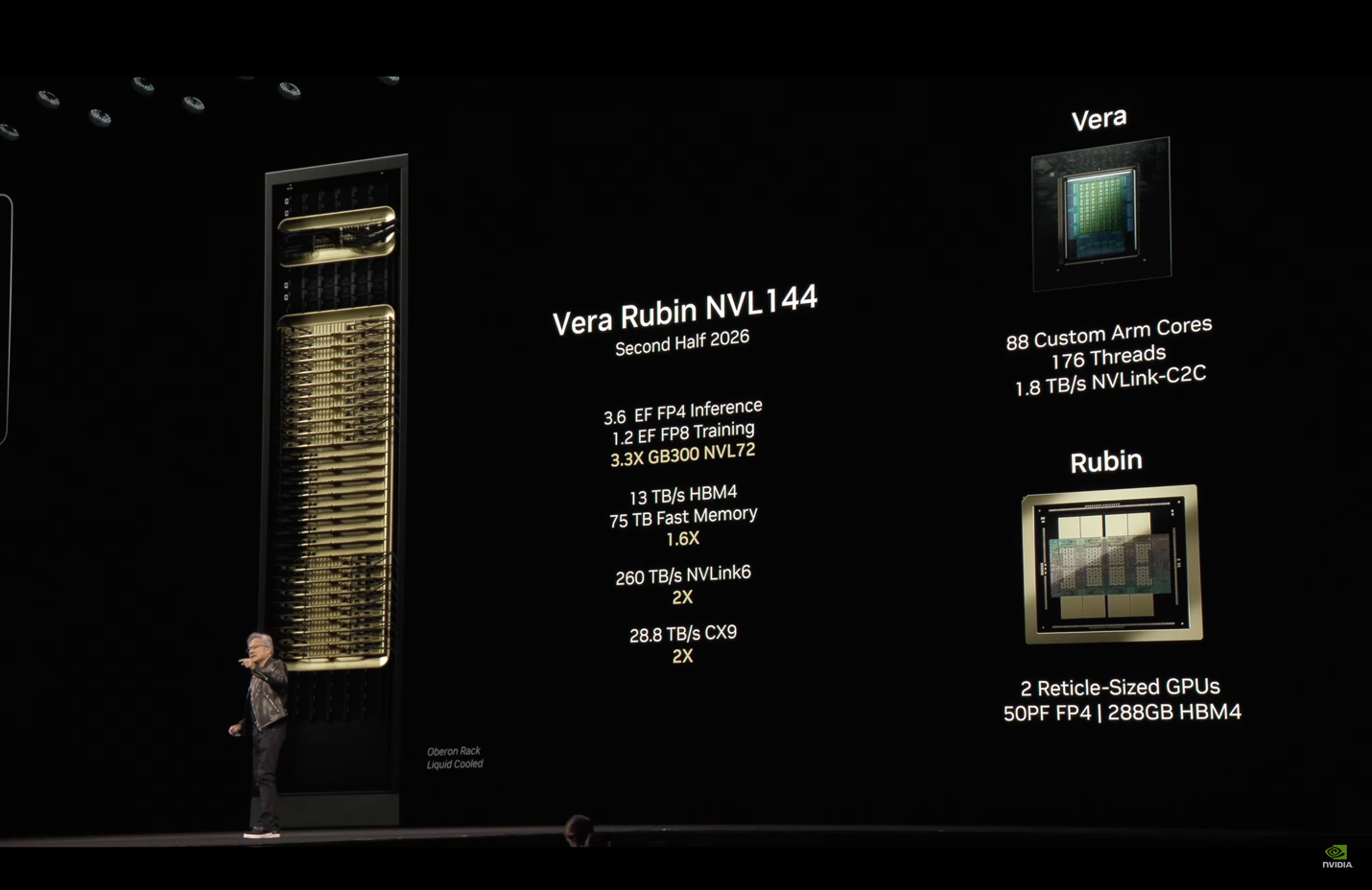
NVIDIA revealing Vera Rubin NVL144 onstage at GTC.
The Vera Rubin NVL144 has 3.6 exaflops of FP4 inference performance, up from 1.1 exaflops for Blackwell Ultra GB300, and 1.2 exaflops of FP8 for training, up from 0.36, which is 3.3x the performance. It’s targeted to ship in the second half of 2026.
Escalating per-rack power requirements are just one of the problems, but the next-generation Rubin Ultra racks are up to 600kW according to Jensen, containing 576 GPUs in 144 modules that each have four Rubin GPUs sharing 1 terabyte of high-bandwidth memory. This is useful information for people designing for data center builds completing 2-3 years out who want to take these next-generation racks. However, it emphasizes that running an AI factory data center is a new set of challenges, even for the hyperscalers and cloud providers, let alone the more traditional enterprise customers.
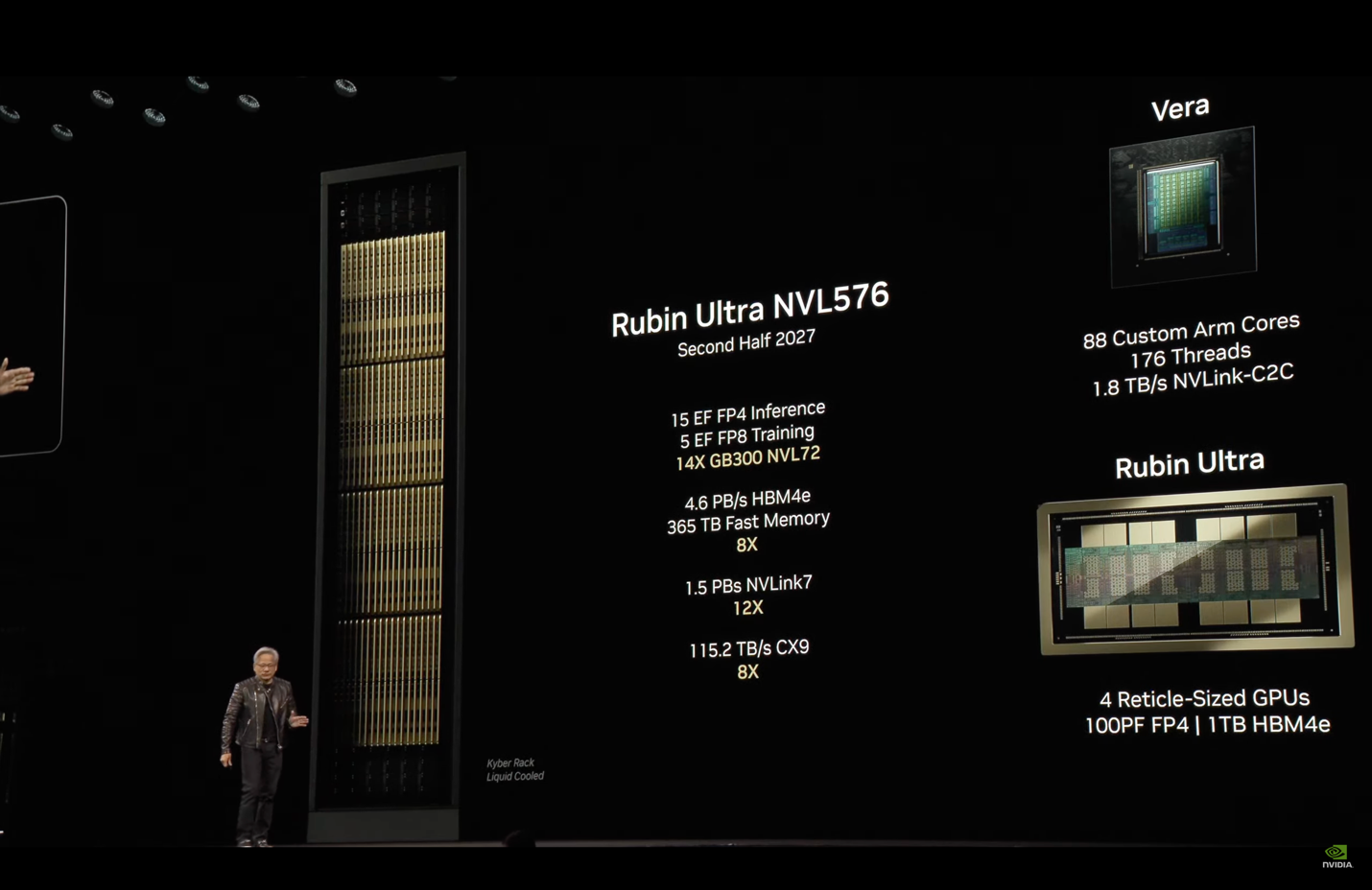
NVIDIA revealing Robin Ultra NVL576 onstage at GTC.
Looking beyond Rubin Ultra in 2027, the next-generation architecture will be named Feynman in 2028, so we can expect to hear more about the performance of that GPU architecture next year.
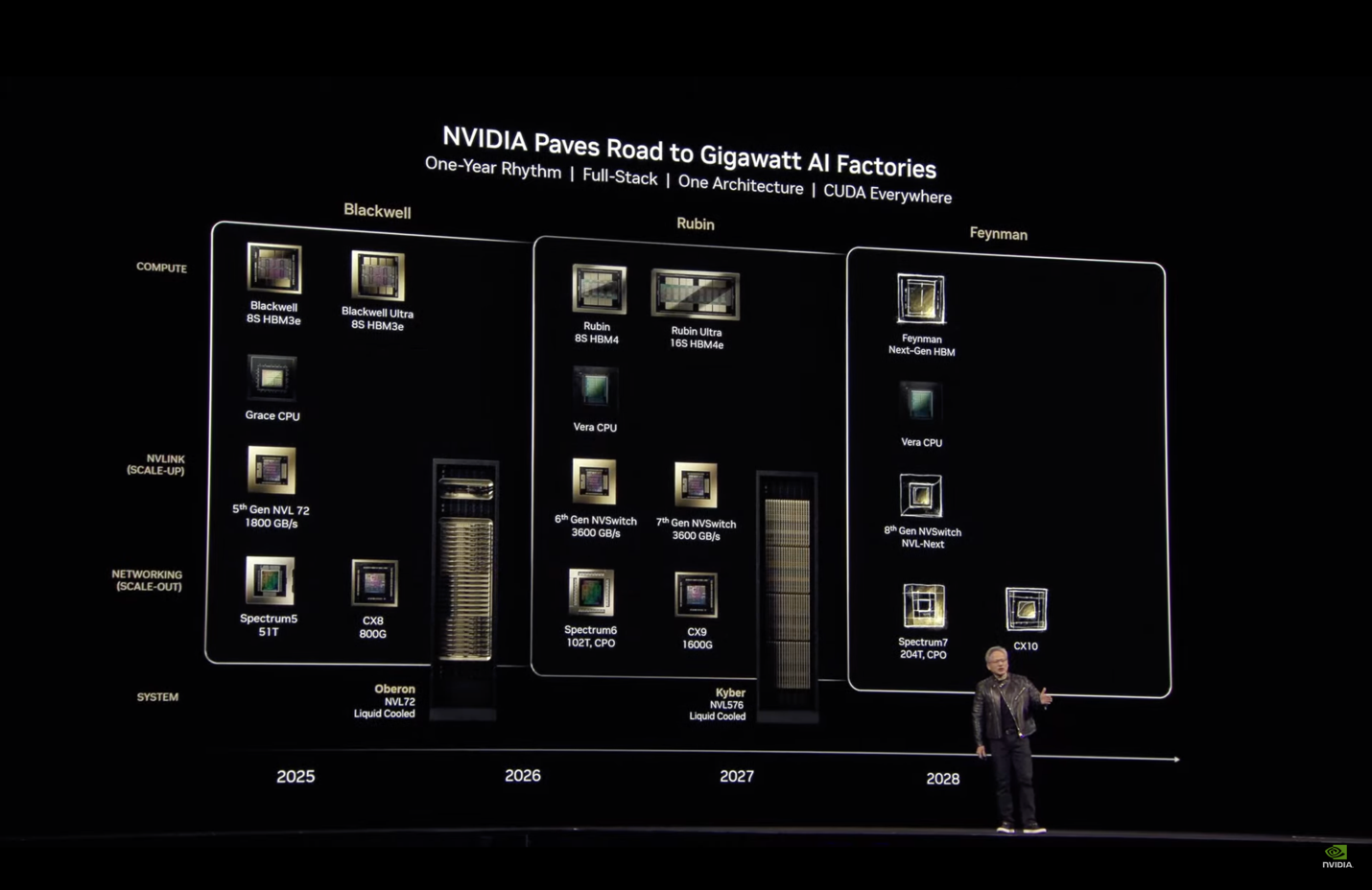
NVIDIA showing its next-gen architecture onstage at GTC.
At the lower end of the scale, NVIDIA is launching a range of desktop and deskside Blackwell-based workstations for the enterprise market. These are particularly useful for accelerated computer-aided engineering (CAE) workloads and Jensen mentioned that many of the standard CAE tools for chip simulation and design, mechanical simulation, etc., are now accelerated.
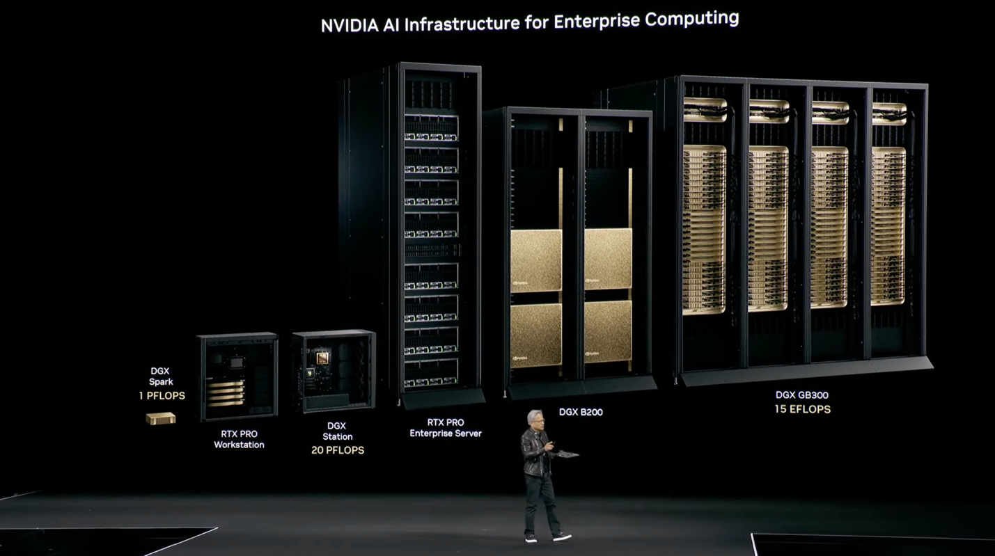
NVIDIA revealing AI infrastructure for enterprise computing onstage at GTC.
Benchmarking
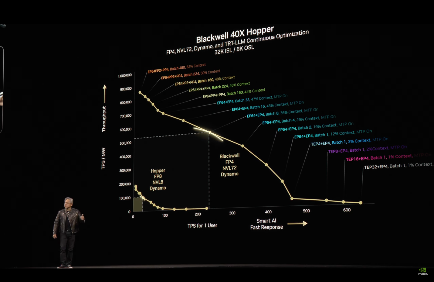
Last year, NVIDIA claimed Blackwell was 4x the performance per GPU for FP8 compared to H100. Blackwell adds a new FP4 capability for inference that doubles the performance and there are additional optimizations for inference that give rise to a 30x improvement claim. I analyzed the 2024 benchmark claims in detail and decided that a more reasonable expectation for configurations of up to eight Blackwell GPUs that most people actually use would be 2.5x the H100 (not 4x) for training, and 8-10x the H100 (not 30x) for inference. These are good improvements in any case. For 2025, the B300 has a 50% increase in raw floating point performance and increased memory capacity to 288GB.
The way Jensen positioned performance was in the context of an AI Factory, which needs to operate in a sweet spot between large efficient batches of work vs. quick responses to interactive queries. That’s where the extra memory and memory bandwidth makes the GPU operate closer to its maximum potential capacity. To further optimize this workload, NVIDIA will release a new open source distributed inference serving library called Dynamo (which isn’t on GitHub as I write this). This helps push the sweet spot further out to have lower interactive latency for larger batches. They are also releasing FP4 optimized open source models.
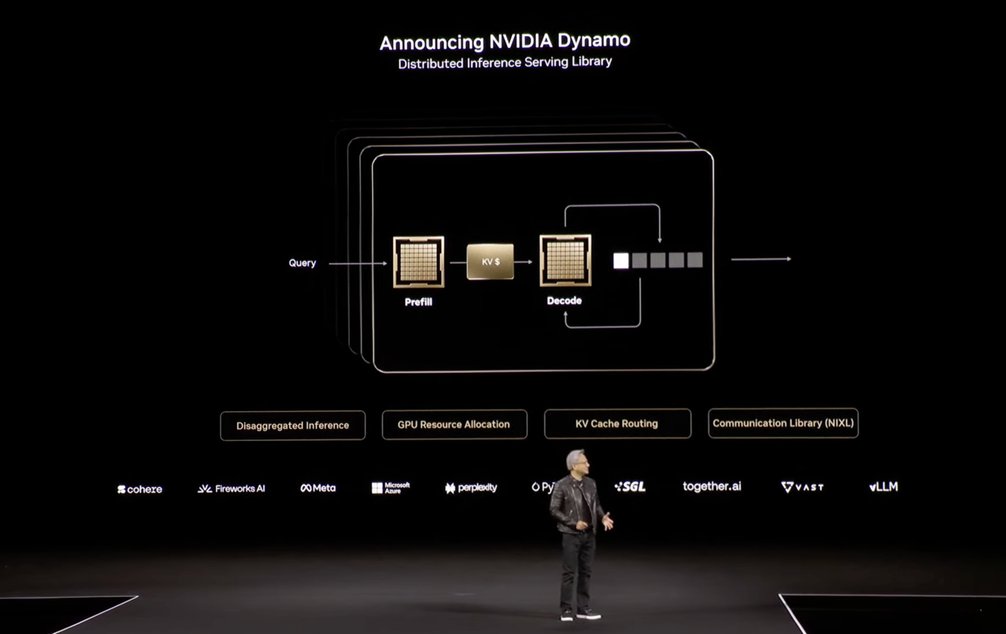
NVIDIA announcing Dynamo onstage at GTC.
The latest performance claim is that with Dynamo and scale-up benefits from the larger NVL72, Blackwell is “40x better” than Hopper at AI Factory hyperscale inference serving. I think the benchmark was explained better this year, than last year, and it’s a relevant application-level benchmark, but I also hope that people don’t assume that a single Blackwell is 30x or 40x faster than a single H100.
Repeated attempts to architect the largest-scale SuperPods at GTC.
Water-Cooled Optical Switches
A big announcement from two years ago was that NVlink could replace the network for up to 256 GH200s combined into a single system connected by 900GB/s interfaces to NVswitch chips. That would have contained 120TB of CPU-hosted memory and 24TB of GPU-hosted high-bandwidth memory, but this configuration seems to have never shipped in volume.
NVlink is a copper-cabling system that operates inside a rack and can reach the next rack over, but won’t reach far enough to build a fully interconnected SuperPod. So in addition to the over-provisioning of CPU capacity with GH200, an additional issue was the high cost of NVlink optical transceivers for building such a big system. For AI training workloads, it’s common to arrange GPUs in a “rail” architecture where they are connected in parallel lines that don’t need to cross-connect. This seems plausible to configure using copper NVlink from one rack to the next on each side, but a system configured this way is only useful for training workloads.
There was an update in 2024 to the shared memory cluster plans, abandoning the GH200 approach and focusing on a GB200-based configuration where the maximum number of GPUs in the shared memory cluster more than doubles from 256 to 576. Again, this seems like a theoretical architecture at this point.
I haven’t been able to find anyone talking about more than 36 or 72 GPUs, and Coreweave’s documentation implies that they configure the NVL72 racks as individual 4-GPU boards networked together. The previously announced deal with AWS to deploy a cluster of GH200s for NVIDIA called Project Ceiba was upgraded (and delayed somewhat) to be a GB200 NVL72-based system with more than 20,000 GPUs instead, as of October 2024. It was not mentioned this year at GTC. I expect that to switch again to be based on GB300 if it’s ever completed.
A key new announcement for 2025 is a very efficient, highly integrated water-cooled optical switch, NVIDIA Photonics. This is going to take out a lot of the complexity, cost and power consumption of larger clusters. The optics terminate directly on the switch chip without needing expensive transceivers. This was probably the biggest surprise announcement in the GTC keynote.
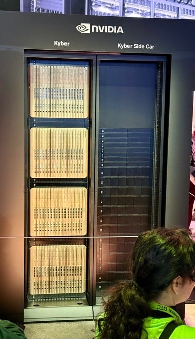
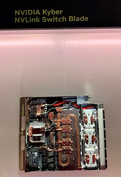
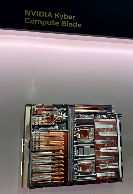
The latest attempt to build a SuperPod appears to be the Rubin NVL576, where the attitude after two previous attempts seems to be, “screw it, put everything in the same rack” and it can all be wired together with low-latency copper cables. This is truly an HPC supercomputer approach, similar to the HP Cray Blackwell rack with 288 GPUs. A prototype of the packaging using Blackwell GPUs and current switch chips was shown in the expo and I took a few pictures.
Can You Afford To Own GPUs?
Same as it ever was. The challenge for customers buying GPUs is that they need to decide what the real useful life of a GPU is before it’s obsolete. It’s far shorter than CPUs, so instead of depreciating like most hardware over 5 or 6 years as seems to be common nowadays, it likely makes sense to depreciate GPUs over 2 or 3 years. That makes them even more expensive to own, and perhaps it’s better to get whatever the latest GPU is available from cloud providers and have them deal with depreciation.
Old GPU capacity tends to end up as a cheap option on a spot market but at some point, it will cost more to power it than it’s worth as a GPU. Jensen said during his keynote that H100 GPUs aren’t generally useful at this point for building AI factories, and sales of Blackwell are much higher than Hopper already.
New Capabilities for Building AI Apps and More
Just like last year, there were many more announcements for markets like robotics, automotive, healthcare, quantum computing, digital twins and cool virtual reality demos that you can watch in the keynote or read about elsewhere, but I’m most impressed by the new GPU hardware specifications and the optical interconnect.
The new stack for AI development has some kind of Blackwell GPU at the base, most likely obtained from one of the GPU cloud vendors like Coreweave rather than AWS or GCP. There’s a CUDA variant for every industry to drive the GPU, the new Dynamo software to operate inference efficiently, optimized models, a large range of third-party packages to get started with and a choice of development tools to help write the remaining code for you.
Jensen started with his favorite slide and I’ll end with it. This is far more than fast hardware: NVIDIA is doing a much better job than its competitors at building the software that makes it easy to build applications and has open sourced most of it. Letting the days go by, once in a lifetime.
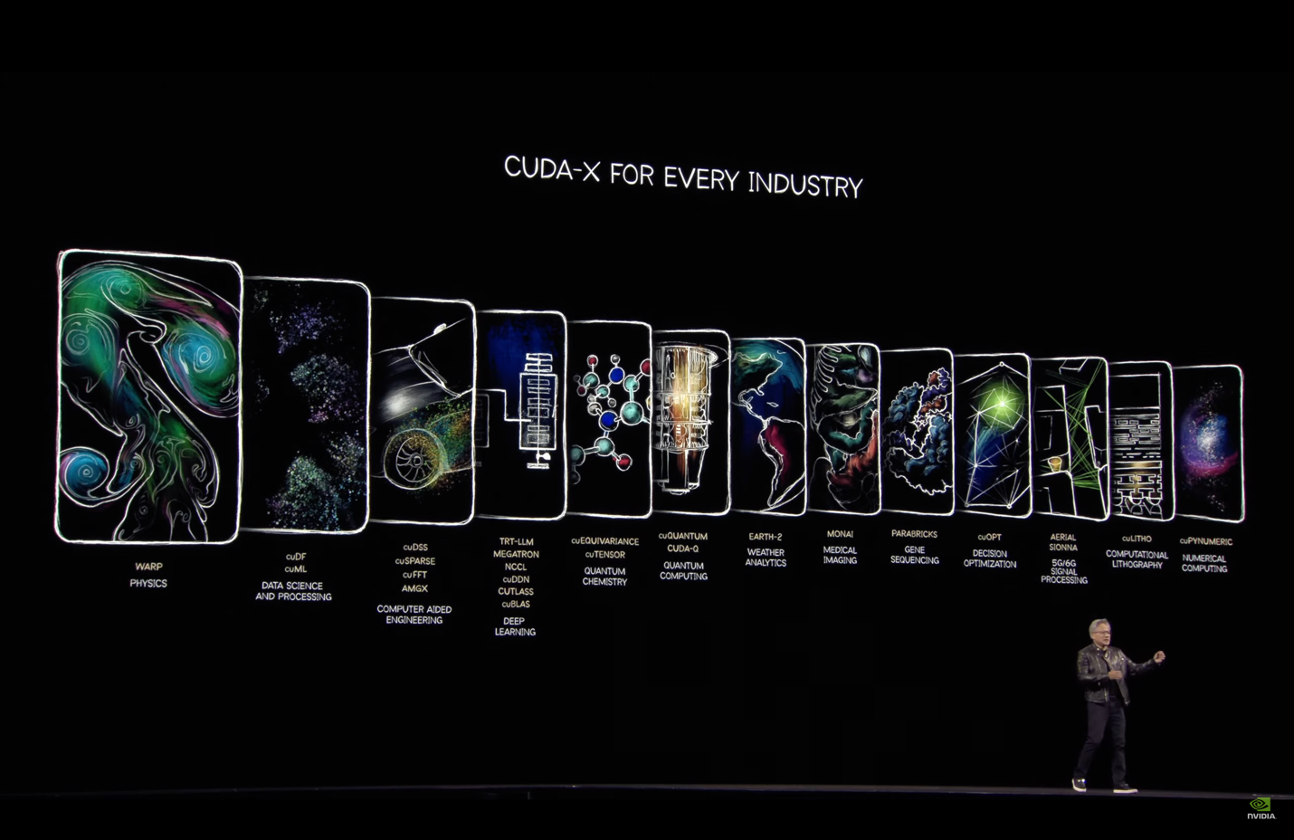
NVIDIA onstage at GTC showing CUDA-X for every industry.
The post NVIDIA Unveils Next-Gen Rubin and Feynman Architectures, Pushing AI Power Limits appeared first on The New Stack.